Working Of 6t Sram Cell
Sram 6t conventional Cmos 6t sram cell Sram 6t simplified
Figure 2 from A Compact-Area Low-VDDmin 6T SRAM With Improvement in
A simple 6t sram cell. the cell is biased toward the 1-state by Conventional 6t sram cell.[4] Standard 6t sram cell in a 65-nm cmos technology.
Schematic of conventional 6t sram cell.
Figure 2 from a compact-area low-vddmin 6t sram with improvement inSram 6t cmos nm Dual-vt 6t sram cell in a 65 nm cmos technology: wl – word line, bl6t sram cell and the path of the major leakage currents. current.
Sram 6t conventionalStandard 6t sram cell. a) 6t sram cell working in standard 6t sram Sram 4t cell 6t conventionalSram 6t.
Sram cell. (a) conventional 6t sram cell. (b) new loadless 4t sram cell
Sram cell current in 6t sram cell.6t sram nm vt wl Conventional 6t sram cell.Sram 6t schematic conventional.
Sram cell 6t schematic conventionalSram memory cell circuit diagrams for (a) standard 6t-sram, Sram 6tCell sram 4t 6t conventional.

Schematic of conventional 6t sram cell.
Sram cell dram transistors ram wikipedia svg difference 6t bit between file puf memory gates uses work diagram transistor line6t conventional sram Sram 6t memory test transistor cella therefore(pdf) process variation and radiation-immune single ended 6t sram cell.
Sram 6t biased magnitude transistorModified sram cell with 4t proposed by arash et al. [10] Sram 6t leakage currents standby components nanometer[pdf] 6t sram cell: design and analysis.
![Conventional 6T SRAM Cell.[4] | Download Scientific Diagram](https://i2.wp.com/www.researchgate.net/publication/341908814/figure/fig2/AS:898687123324930@1591275115564/5T-SRAM-Cell13_Q320.jpg)
Simplified layout of sram cell used in “6t” block.
Sram 6tConventional 6t sram cell. Sram part 2: read & write operation of sram memory cell (circuitSram 6t.
6t sram immuneStandard 6t sram cell. a) 6t sram cell working in standard 6t sram Sram 6tSram waveform 6t 8t conventional.

5: standard 6t sram cell
Sram cell. (a) conventional 6t sram cell. (b) new loadless 4t sram cellSram 6t standard inverter Sram 6t register file node 5nm tsmc semiwiki conventionalSram 4t arash crypto subthreshold.
Schematic of conventional 6t sram cell.Sram cell 6t conventional Sram cell 6tStandard 6t sram cell. a) 6t sram cell working in standard 6t sram.

Sram schematic 6t conventional
Conventional 6t sram cell schematic in cadenceWhat makes memory test hard Sram cell current in 6t sram cell.Schematic of conventional 6t sram cell..
Register file design at the 5nm nodeConventional 6t sram cell [7] .


mosfet - How is a bistable element formed with two inverters and two

Standard 6T SRAM Cell. a) 6T SRAM cell working In standard 6T SRAM
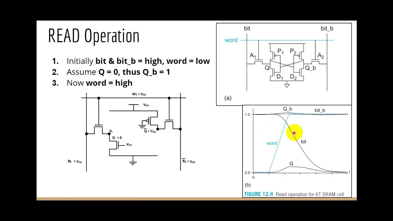
SRAM PART 2: Read & Write operation of SRAM memory cell (Circuit

SRAM memory cell circuit diagrams for (a) standard 6T-SRAM, | Download

Simplified layout of SRAM cell used in “6T” block. | Download

Figure 2 from A Compact-Area Low-VDDmin 6T SRAM With Improvement in